Non-uniform memory access (NUMA) is a shared memory architecture used in today’s multiprocessing systems. Each CPU is assigned its own local memory and can access memory from other CPUs in the system. Local memory access provides a low latency – high bandwidth performance. While accessing memory owned by the other CPU has higher latency and lower bandwidth performance. Modern applications and operating systems such as ESXi support NUMA by default, yet to provide the best performance, virtual machine configuration should be done with the NUMA architecture in mind. If incorrect designed, inconsequent behavior or overall performance degradation occurs for that particular virtual machine or in worst case scenario for all VMs running on that ESXi host.
This series aims to provide insights of the CPU architecture, the memory subsystem and the ESXi CPU and memory scheduler. Allowing you in creating a high performing platform that lays the foundation for the higher services and increased consolidating ratios. Before we arrive at modern compute architectures, it’s helpful to review the history of shared-memory multiprocessor architectures to understand why we are using NUMA systems today.
The evolution of shared-memory multiprocessors architecture in the last decades
It seems that an architecture called Uniform Memory Access would be a better fit when designing a consistent low latency, high bandwidth platform. Yet modern system architectures will restrict it from being truly uniform. To understand the reason behind this we need to go back in history to identify the key drivers of parallel computing.
With the introduction of relational databases in the early seventies the need for systems that could service multiple concurrent user operations and excessive data generation became mainstream. Despite the impressive rate of uniprocessor performance, multiprocessor systems were better equipped to handle this workload. In order to provide a cost-effective system, shared memory address space became the focus of research. Early on, systems using a crossbar switch were advocated, however with this design complexity scaled along with the increase of processors, which made the bus-based system more attractive. Processors in a bus system are allowed to access the entire memory space by sending requests on the bus, a very cost effective way to use the available memory as optimally as possible.
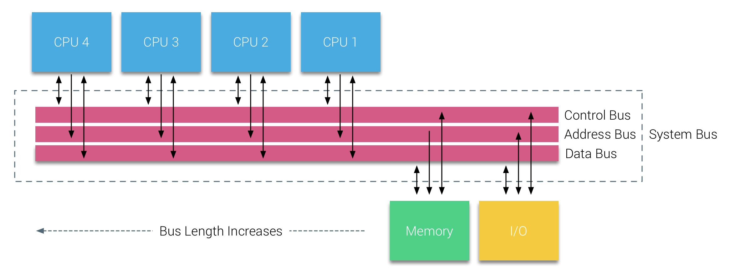
However, bus-based systems have their own scalability problems. The main issue is the limited amount of bandwidth, this restrains the number of processors the bus can accommodate. Adding CPUs to the system introduces two major areas of concern:
- The available bandwidth per node decreases as each CPU added.
- The bus length increases when adding more processors, thereby increasing latency.
The performance growth of CPU and specifically the speed gap between the processor and the memory performance was, and actually still is, devastating for multiprocessors. Since the memory gap between processor and memory was expected to increase, a lot of effort went into developing effective strategies to manage the memory systems. One of these strategies was adding memory cache, which introduced a multitude of challenges. Solving these challenges is still the main focus of today for CPU design teams, a lot of research is done on caching structures and sophisticated algorithms to avoid cache misses.
Introduction of caching snoop protocols
Attaching a cache to each CPU increases performance in many ways. Bringing memory closer to the CPU reduces the average memory access time and at the same time reducing the bandwidth load on the memory bus. The challenge with adding cache to each CPU in a shared memory architecture is that it allows multiple copies of a memory block to exist. This is called the cache-coherency problem. To solve this, caching snoop protocols were invented attempting to create a model that provided the correct data while not trying to eat up all the bandwidth on the bus. The most popular protocol, write invalidate, erases all other copies of data before writing the local cache. Any subsequent read of this data by other processors will detect a cache miss in their local cache and will be serviced from the cache of another CPU containing the most recently modified data. This model saved a lot of bus bandwidth and allowed for Uniform Memory Access systems to emerge in the early 1990s. Modern cache coherency protocols are covered in more detail by part 3.
Uniform Memory Access Architecture
Processors of Bus-based multiprocessors that experience the same – uniform – access time to any memory module in the system are often referred to as Uniform Memory Access (UMA) systems or Symmetric Multi-Processors (SMPs).
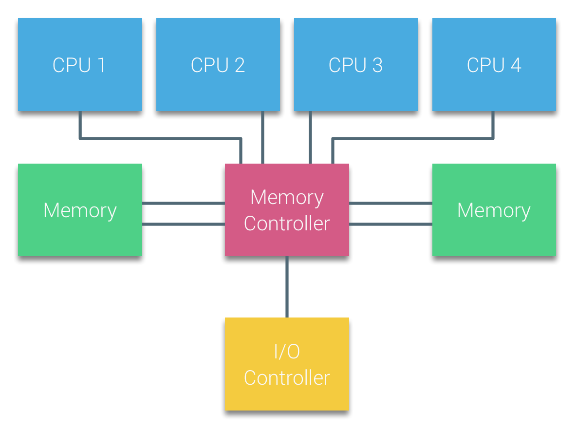
With UMA systems, the CPUs are connected via a system bus (Front-Side Bus) to the Northbridge. The Northbridge contains the memory controller and all communication to and from memory must pass through the Northbridge. The I/O controller, responsible for managing I/O to all devices, is connected to the Northbridge. Therefore, every I/O has to go through the Northbridge to reach the CPU.
Multiple buses and memory channels are used to double the available bandwidth and reduce the bottleneck of the Northbridge. To increase the memory bandwidth even further some systems connected external memory controllers to the Northbridge, improving bandwidth and support of more memory. However due the internal bandwidth of the Northbridge and the broadcasting nature of early snoopy cache protocols, UMA was considered to have a limited scalability. With today’s use of high-speed flash devices, pushing hundreds of thousands of IO’s per second, they were absolutely right that this architecture would not scale for future workloads.
Non-Uniform Memory Access Architecture
To improve scalability and performance three critical changes are made to the shared-memory multiprocessors architecture;
- Non-Uniform Memory Access organization
- Point-to-Point interconnect topology
- Scalable cache coherence solutions
1: Non-Uniform Memory Access organization
NUMA moves away from a centralized pool of memory and introduces topological properties. By classifying memory location bases on signal path length from the processor to the memory, latency and bandwidth bottlenecks can be avoided. This is done by redesigning the whole system of processor and chipset. NUMA architectures gained popularity at the end of the 90’s when it was used on SGI supercomputers such as the Cray Origin 2000. NUMA helped to identify the location of the memory, in this case of these systems, they had to wonder which memory region in which chassis was holding the memory bits.
In the first half of the millennium decade, AMD brought NUMA to the enterprise landscape where UMA systems reigned supreme. In 2003 the AMD Opteron family was introduced, featuring integrated memory controllers with each CPU owning designated memory banks. Each CPU has now its own memory address space. A NUMA optimized operating system such as ESXi allows workload to consume memory from both memory addresses spaces while optimizing for local memory access. Let’s use an example of a two CPU system to clarify the distinction between local and remote memory access within a single system.
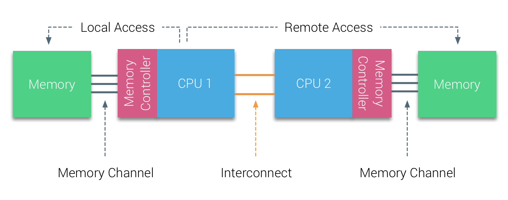
The memory connected to the memory controller of the CPU1 is considered to be local memory. Memory connected to another CPU socket (CPU2)is considered to be foreign or remote for CPU1. Remote memory access has additional latency overhead to local memory access, as it has to traverse an interconnect (point-to-point link) and connect to the remote memory controller. As a result of the different memory locations, this system experiences “non-uniform” memory access time.
2: Point-to-Point interconnect
AMD introduced their point-to-point connection HyperTransport with the AMD Opteron microarchitecture. Intel moved away from their dual independent bus architecture in 2007 by introducing the QuickPath Architecture in their Nehalem Processor family design.
The Nehalem architecture was a significant design change within the Intel microarchitecture and is considered the first true generation of the Intel Core series. The current Broadwell architecture is the 4th generation of the Intel Core brand (Intel Xeon E5 v4), the last paragraph contains more information on the microarchitecture generations. Within the QuickPath architecture, the memory controllers moved to the CPU and introduced the QuickPath point-to-point Interconnect (QPI) as data-links between CPUs in the system.
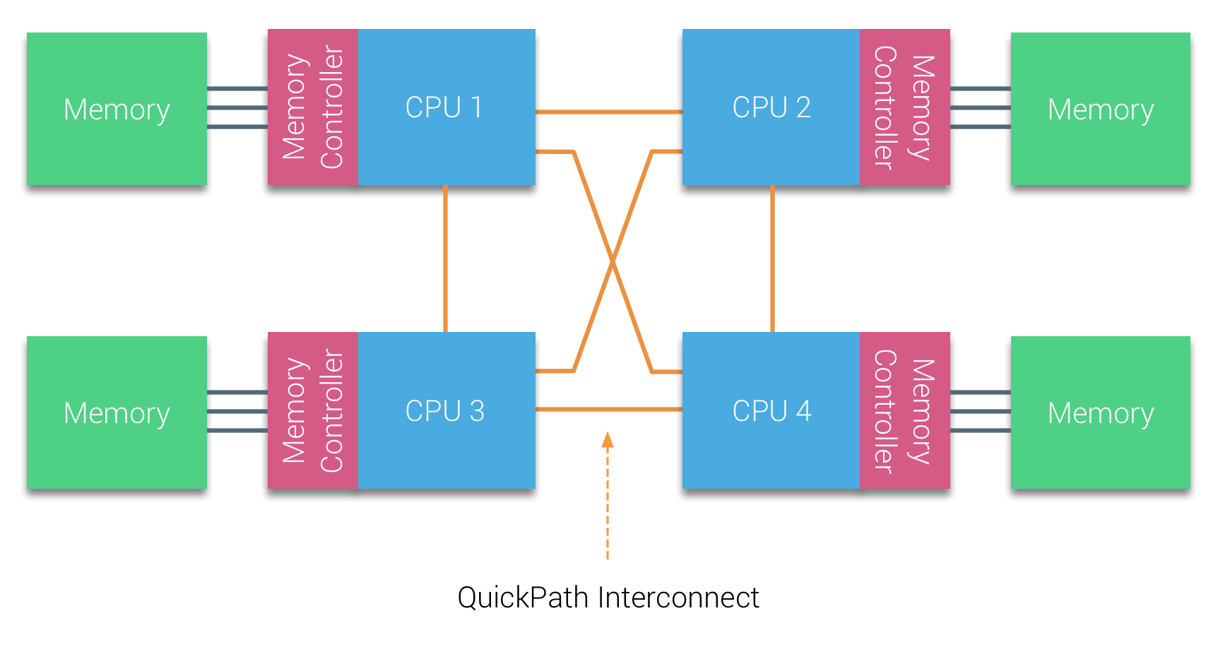
The Nehalem microarchitecture not only replaced the legacy front-side bus but reorganized the entire sub-system into a modular design for server CPU. This modular design was introduced as the “Uncore” and creates a building block library for caching and interconnect speeds. Removing the front-side bus improves bandwidth scalability issues, yet intra- and inter-processor communication have to be solved when dealing with enormous amounts of memory capacity and bandwidth. Both the integrated memory controller and the QuickPath Interconnects are a part of the Uncore and are Model Specific Registers (MSR) ). They connect to a MSR that provides the intra- and inter-processor communication. The modularity of the Uncore also allows Intel to offer different QPI speeds, at the time of writing the Intel Broadwell-EP microarchitecture (2016) offers 6.4 Giga-transfers per second (GT/s), 8.0 GT/s and 9.6 GT/s. Respectively providing a theoretical maximum bandwidth of 25.6 GB/s, 32 GB/s and 38.4 GB/s between the CPUs. To put this in perspective, the last used front-side bus provided 1.6 GT/s or 12.8 GB/s of platform bandwidth. When introducing Sandy Bridge Intel rebranded Uncore into System Agent, yet the term Uncore is still used in current documentation. You can find more about QuickPath and the Uncore in part 2.
3: Scalable Cache Coherence
Each core had a private path to the L3 cache. Each path consisted of a thousand wires and you can imagine this doesn’t scale well if you want to decrease the nanometer manufacturing process while also increasing the cores that want to access the cache. In order to be able to scale, the Sandy Bridge Architecture moved the L3 cache out of the Uncore and introduced the scalable ring on-die Interconnect. This allowed Intel to partition and distribute the L3 cache in equal slices. This provides higher bandwidth and associativity. Each slice is 2.5 MB and one slice is associated with each core. The ring allows each core to access every other slice as well. Pictured below is the die configuration of a Low Core Count (LCC) Xeon CPU of the Broadwell Microarchitecture (v4) (2016).
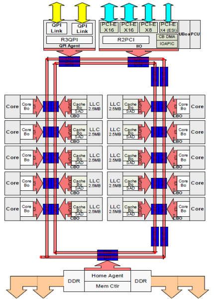
This caching architecture requires a snooping protocol that incorporates both distributed local cache as well as the other processors in the system to ensure cache coherency. With the addition of more cores in the system, the amount of snoop traffic grows, since each core has its own steady stream of cache misses. This affects the consumption of the QPI links and last level caches, requiring ongoing development in snoop coherency protocols. An in-depth view of the Uncore, scalable ring on-Die Interconnect and the importance of caching snoop protocols on NUMA performance will be included in part 3.
Non-interleaved enabled NUMA = SUMA
Physical memory is distributed across the motherboard, however, the system can provide a single memory address space by interleaving the memory between the two NUMA nodes. This is called Node-interleaving (setting is covered in part 2). When node interleaving is enabled, the system becomes a Sufficiently Uniform Memory Architecture (SUMA). Instead of relaying the topology info and nature of the processors and memory in the system to the operating system, the system breaks down the entire memory range into 4KB addressable regions and maps them in a round robin fashion from each node. This provides an ‘interleaved’ memory structure where the memory address space is distributed across the nodes. When ESXi assigns memory to virtual machine it allocates physical memory located from two different nodes when the physical CPU located in Node 0 needs to fetch the memory from Node 1, the memory will traverse the QPI links.
The interesting thing is that the SUMA system provides a uniform memory access time. Only not the most optimal one and heavily depends on contention levels in the QPI architecture. Intel Memory Latency Checker was used to demonstrate the differences between NUMA and SUMA configuration on the same system.
This test measures the idle latencies (in nanoseconds) from each socket to the other socket in the system. The latency reported of Memory Node 0 by Socket 0 is local memory access, memory access from socket 0 of memory node 1 is remote memory access in the system configured as NUMA.
| NUMA | Memory Node 0 | Memory Node 1 | – | SUMA | Memory Node 0 | Memory Node 1 |
| Socket 0 | 75.7 | 132.0 | – | Socket 0 | 105.5 | 106.4 |
| Socket 1 | 131.9 | 75.8 | – | Socket 1 | 106.0 | 104.6 |
As expected interleaving is impacted by constant traversing the QPI links. The idle memory test is the best case scenario, a more interesting test is measuring loaded latencies. It would have been a bad investment if your ESXi servers are idling, therefor you can assume that an ESXi system is processing data. Measuring loaded latencies provides a better insight on how the system will perform under normal load. During the test the load injection delays are automatically changed every 2 seconds and both the bandwidth and the corresponding latency is measured at that level. This test uses 100% read traffic.NUMA test results on the left, SUMA test results on the right.
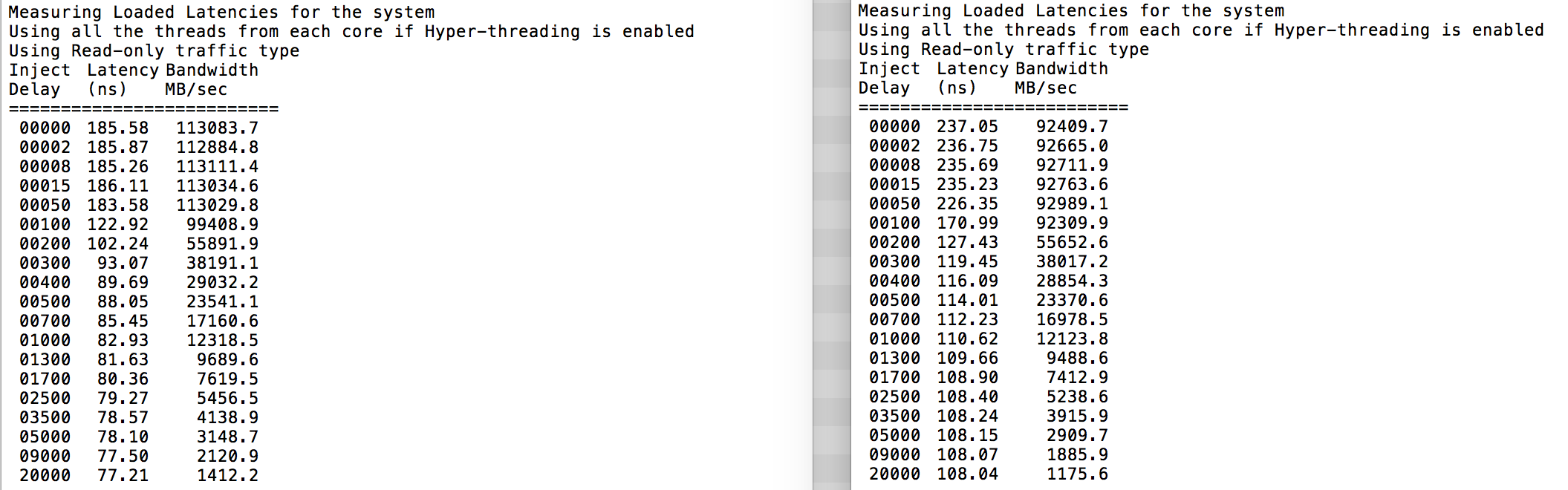
The reported bandwidth for the SUMA system is lower while maintaining a higher latency than the system configured as NUMA. Therefore, the focus should be on optimizing the VM size to leverage the NUMA characteristics of the system.
Nehalem & Core microarchitecture overview
With the introduction of the Nehalem microarchitecture in 2008, Intel moved away from the Netburst architecture. The Nehalem microarchitecture introduced Intel customers to NUMA. Along the years Intel introduced new microarchitectures and optimizations, according to its famous Tick-Tock model. With every Tick, optimization takes place, shrinking the process technology and with every Tock a new microarchitecture is introduced. Even though Intel provides a consistent branding model since 2012, people tend to Intel architecture codenames to discuss the CPU tick and tock generations. Even the EVC baselines lists these internal Intel codenames, both branding names and architecture codenames will be used throughout this series:
| Microarchitecture DP servers | Branding | Year | Cores | LLC (MB) | QPI Speed (GT/s) | Memory Frequency | Architectural change | Fabrication Process |
| Nehalem | x55xx | 10-2008 | 4 | 8 | 6.4 | 3xDDR3-1333 | Tock | 45nm |
| Westmere | x56xx | 01-2010 | 6 | 12 | 6.4 | 3xDDR3-1333 | Tick | 32nm |
| Sandy Bridge | E5-26xx v1 | 03-2012 | 8 | 20 | 8.0 | 4xDDR3-1600 | Tock | 32nm |
| Ivy Bridge | E5-26xx v2 | 09-2013 | 12 | 30 | 8.0 | 4xDDR3-1866 | Tick | 22 nm |
| Haswell | E5-26xx v3 | 09-2014 | 18 | 45 | 9.6 | 4xDDR3-2133 | Tock | 22nm |
| Broadwell | E5-26xx v4 | 03-2016 | 22 | 55 | 9.6 | 4xDDR3-2400 | Tick | 14 nm |
Up next, Part 2: System Architecture
The 2016 NUMA Deep Dive Series:
Part 0: Introduction NUMA Deep Dive Series
Part 1: From UMA to NUMA
Part 2: System Architecture
Part 3: Cache Coherency
Part 4: Local Memory Optimization
Part 5: ESXi VMkernel NUMA Constructs

you just fucked my brain with this amazing post.. now i feel i am relaxed
I thought I knew pretty much about NUMA, but turns out I knew nothing. Awesome deep dive, Thanks a lot.
Question – how does SUMA manage to provide a uniform memory access time? I thought the access time difference between NUMA and SUMA was a physical characteristic difference due to number of hops between cores and memory banks and due to different bandwidth/latency specs of local memory channels vs QPI.
And thanks for tick&tock explanation – that was pretty interesting.
@Askar
As Frank as explained – the logical memory addressing in sequence is interleaved or round robin-ed between the physical memory locations(nodes). Eg: Assuming a two CPU system (2 nodes)
Logical memory address 0 – on node 0
Logical memory address 1 – on node 1
Logical memory address 3 – on node 0
Logical memory address 4 – on node 1 ….
So the law of averages – some address will be super quick and some not as the requested memory location as to mapped to the physical location (node).
If you use the table frank provides – Socket 0 memory 0 = 75.7 memory 1 = 132.0 (memory 0 is local, 1 remote)
75.7 + 132.0 = 207.7 / 2 == 103.85 very close the the SUMA score of 105.5 & 106.4.
Hope this help explains it.
Phil
@the_vMonkey
Hi Phil,
yes, that makes sense.
I think I got confused by the table with SUMA nodes memory access latency numbers. The table looks like even with node interleaving enabled each core was testing local and remote access separately, however, the core was actually accessing two different memory banks in round-robin fashion.
Thanks for the explanation.
@askar Well, they are using 2 CPU system, so effectively, you place half the memory on one CPU and half on the other (we are talking about memory we are utilizing, not the RAM itself). So your application accesses memory from CPU1 as equally as memory from CPU2 (well, if its truly random). At least that’s how I understood it. I might be wrong.
The point been made is that SUMA is like a ‘lazy’ admins fix or if the Operating system does not understand NUMA and it underlying CPU/RAM infrastructure. If using NUMA and don’t take not of it you could have a case of two VMs – that have total different performance – eg VM 1 as its confg mapped to a single node – thus ram is local. Another might have ram that is split across nodes.
Great post, thanks for sharing.
I’ve never thought of it before, but it almost tells a story of why HCI *may* be the future. That is HCI = NUMA and shared storage = UMA. I don’t think the bandwidth and latency limitations are any where near as constrained in storage as they are in a CPU, but an interesting similarity none the less.
Broadwell E5-26xx v4 03-2016 22 55 9.6 4xDDR3-2400 Tick 14 nm
With E5-26xx v4 it’s DDR4 and not DDR3
thanks for spotting the typo