Reviewing the physical layers helps to understand the behavior of the CPU scheduler of the VMkernel. This helps to select a physical configuration that is optimized for performance. This part covers the Intel Xeon microarchitecture and zooms in on the Uncore. Primarily focusing on Uncore frequency management and QPI design decisions.
Terminology
There a are a lot of different names used for something that is apparently the same thing. Let’s review the terminology of the Physical CPU and the NUMA architecture. The CPU package is the device you hold in your hand, it contains the CPU die and is installed in the CPU socket on the motherboard. The CPU die contains the CPU cores and the system agent. A core is an independent execution unit and can present two virtual cores to run simultaneous multithreading (SMT). Intel proprietary SMT implementation is called Hyper-Threading (HT). Both SMT threads share the components such as cache layers and access to the scalable ring on-die Interconnect for I/O operations.

Interesting entomology; The word “die” is the singular of dice. Elements such as processing units are produced on a large round silicon wafer. The wafer is cut “diced” into many pieces. Each of these pieces is called a die.
NUMA Architecture
In the following scenario, the system contains two CPUs, Intel 2630 v4, each containing 10 cores (20 HT threads). The Intel 2630 v4 is based on the Broadwell microarchitecture and contains 4 memory channels, with a maximum of 3 DIMMS per channel. Each channel is filled with a single 16 GB DDR4 RAM DIMM. 64 GB memory is available per CPU with a total of 128 GB in the system. The system reports two NUMA Nodes, each NUMA nodes, sometimes called NUMA domain, contains 10 cores and 64 GB.

Consuming NUMA
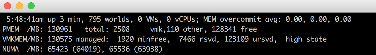
The CPU can access both its local memory and the memory controlled by the other CPUs in the system. Memory capacity managed by other CPUs are considered remote memory and is accessed through the QPI (Part 1). The allocation of memory to a virtual machine is handled by the CPU and NUMA schedulers of the ESXi kernel. The goal of the NUMA scheduler is to maximize local memory access and attempts to distribute the workload as efficient as possible. This depends on the virtual machine CPU and memory configuration and the physical core count and memory configuration. A more detailed look into the behavior of the ESXi CPU and NUMA scheduler is done in part 5, how to size and configure your virtual machines is discussed in part 6. This part focusses on the low-level configuration of a modern dual-CPU socket system. ESXtop reports 130961 MB (PMEM /MB) and displays the NUMA nodes with its local memory count.
Each core can address up to 128 GB of memory, as described earlier the NUMA scheduler of the ESXI kernel attempts to place and distribute vCPU as optimal as possible, allocating as much local memory to the CPU workload that is available. When the number of VCPUs of a virtual machine exceeds the core count of a physical CPU, the ESXi server distributes the vCPU even across the minimal number of physical CPUs.It also exposes the physical NUMA layout to the virtual machine operating system, allowing the NUMA-aware operating system and / or application to schedule their processes as optimal as possible. To ensure this all occurs, verify if the BIOS is configured correctly and that the setting NUMA = enabled or Node Interleaving is disabled. In this example a 12 vCPU VM is running on the dual Intel 2630 v4 system, each containing 10 cores. CoreInfo informs us that 6 vCPUs are running on NUMA node 0 and 6 vCPUs are running on NUMA node 1.

BIOS Setting: Node Interleaving
There seems to be a lot of confusion about this BIOS setting, I receive lots of questions on whether to enable or disable Node interleaving. I guess the term “enable” make people think it some sort of performance enhancement. Unfortunately, the opposite is true and it is strongly recommended to keep the default setting and keep Node Interleaving disabled.
Node Interleaving Disabled: NUMA
By using the default setting of Node Interleaving (disabled), the ACPI “BIOS” will build a System Resource Allocation Table (SRAT). Within this SRAT, the physical configuration and CPU memory architecture are described, i.e. which CPU and memory ranges belong to a single NUMA node. It proceeds to map the memory of each node into a single sequential block of memory address space. ESXi uses the SRAT to understand which memory bank is local to a physical CPU and attempts to allocate local memory to each vCPU of the virtual machine.
Node Interleaving Enabled: SUMA
One question that is asked a lot is how do you turn off NUMA? You can turn off NUMA, but remember your system is not a transformer, changing your CPUs and memory layout from a point-to-point-connection architecture to a bus system. Therefore, when enabling Node Interleaving the system will not become a traditional UMA system. Part 1 contains a more info on SUMA.
BIOS setting: ACPI SLIT Preferences
The ACPI System Locality Information Table (SLIT) provides a matrix that describes the relative distance (i.e. memory latency) between the proximity domains. In the past, a large NUMA system the latency from Node 0 to Node 7 can be much greater than the latency from Node 0 to Node 1, and this kind of information is provided by the SLIT table.
Modern point-to-point architectures moved from a ring topology to a full mesh topology reducing hop counts, reducing the importance of SLIT. Many server vendor whitepapers describing best practices for VMware ESXi recommend enabling ACPI SLIT. Do not worry if you forgot to enable this setting as ESXi does not use the SLIT. Instead, the ESXi kernel determines the inter-node latencies by probing the nodes at boot-time and use this information for initial placement of wide virtual machines. A wide virtual machine contains more vCPUs than the Core count of a physical CPU, more about wide virtual machines and virtual NUMA can be found in the next article.
CPU System Architecture
Since Sandy Bridge (v1) the CPU system architecture applied by Intel can be described as a System-on-Chip (SoC) architecture, integrating the CPU, GPU, system IO and last level cache into a single package. The QPI and the Uncore are critical components of the memory system and its performance can be impacted by BIOS settings. Available QPI bandwidth depends on the CPU model, therefore it’s of interest to have a proper understanding of the CPU system architecture to design a high performing system.
Uncore
As mentioned in part 1, the Nehalem microarchitecture introduced a flexible architecture that could be optimized for different segments. In order to facilitate scalability, Intel separated the core processing functionality (ALU, FPU, L1 and L2 cache) from the ‘uncore’ functionality. A nice way to put it is that the Uncore is a collection of components of a CPU that do not carry out core computational functions but are essential for core performance. This architectural system change brought the Northbridge functionality closer to the processing unit, reducing latency while being able to increase the speed due to the removal of serial bus controllers. The Uncore featured the following elements:
| Uncore element | Description | Responsible for: |
|---|---|---|
| QPI Agent | QuickPath Interconnect | QPI caching agent , manages R3QPI and QPI Link Interface |
| PCU | Power Controller | Core/Uncore power unit and thermal manager, governs P-state of the CPU, C-state of the Core and package. It enables Turbo Mode and can throttle cores when a thermal violation occurs |
| Ubox | System Config controller | Intermediary for interrupt traffic between system and core |
| IIO | Integrated IO | Provides the interface to PCIe Devices |
| R2PCI | Ring to PCI Interface | Provides interface to the ring for PCIe access |
| IMC | Integrated Memory Controller | Provides the interface to RAM and communicates with Uncore through home agent |
| HA | Integrated Memory Controller | Provides the interface to RAM and communicates with Uncore through home agent |
| SMI | Scalable Memory Interface | Provides IMC access to DIMMs |
Intel provides a schematic overview of a CPU to understand the relationship between the Uncore and the cores, I’ve recreated this overview to help emphasise certain components. Please note that the following diagram depicts a High Core Count architecture of the Intel Xeon v4 (Broadwell). This is a single CPU package. The cores are spread out in a “chop-able” design, allowing Intel to offer three different core counts, Low, Medium and High. The red line is depicting the scalable on-die ring connecting the cores with the rest of the Uncore components. More in-depth information can be found in part 4 of this series.

If a CPU core wants to access data it has to communicate with the Uncore. Data can be in the last-level cache (LLC), thus interfacing with the Cbox, it might require memory from local memory, interfacing with the home agent and integrated memory controller (IMC). Or it needs to fetch memory from a remote NUMA node, as a consequence, the QPI comes into play. Due to the many components located in the Uncore, it plays a significant part in the overall power consumption of the system. With today’s focus on power reduction, the Uncore is equipped with frequency scaling functionality (UFS).
Haswell (v4) introduces Per Core Power States (PCPS) that allows each core to run at its own frequency. UFS allows the Uncore components to scale their frequency up and down independently of the cores. This allows Turbo Boost 2.0 to turbo up and owns the two elements independently, allowing cores to scale up the frequency of their LLC and ring on-ramp modules, without having to enforce all Uncore elements to turbo boost up and waste power. The feature that regulates boosting of the two elements is called Energy Efficient Turbo, some vendors provide the ability to manage power consumption with the settings Uncore Frequency Override or Uncore Frequency. These settings are geared towards applying performance savings in a more holistic way.
The Uncore provides access to all interfaces, plus it regulates the power states of the cores, therefore it has to be functional even when there is a minimal load on the CPU. To reduce overall CPU power consumption, the power control mechanism attempts to reduce the CPU frequency to a minimum by using C1E states on separate cores. If a C1E state occurs, the frequency of the Uncore is likely to be lowered as well. This could have a negative effect on the I/O throughput of the overall throughput of the CPU. To avoid this from happening some server vendors provide the BIOS option; Uncore Frequency Override. By default this option is set to Disabled, allowing the system to reduce the Uncore frequency to obtain power consumption savings. By selecting Enabled it prevents frequency scaling of the Uncore, ensuring high performance. To secure high levels of throughput of the QPI links, select the option enabled, keep in mind that this can have a negative (increased) effect on the power consumption of the system.
Some vendors provide the Uncore Frequency option of Dynamic and Maximum. When set to Dynamic, the Uncore frequency matches the frequency of the fastest core. With most server vendors, when selecting the dynamic option, the optimization of the Uncore frequency is to save power or to optimize the performance. The bias towards power saving and optimize performance is influenced by the setting of power-management policies. When the Uncore frequency option is set to maximum the frequency remains fixed.
Generally, this modularity should make it more power efficient, however, some IT teams don’t want their system to swing up and down but provide a consistent performance. Especially when the workload is active across multiple nodes in a cluster, running the workload consistently is more important that having a specific node to go as fast as it can.
Quick Path Interconnect Link
Virtual machine configuration can impact memory allocation, for example when the memory configuration consumption exceeds the available amount of local memory, ESXi allocates remote memory to this virtual machine. An imbalance of VM activity and VM resource consumption can trigger the ESXi host to rebalance the virtual machines across the NUMA nodes which lead to data migration between the two NUMA nodes. These two examples occur quite frequently, as such the performance of remote memory access, memory migration, and low-level CPU processes such as cache snooping and validation traffic depends on the QPI architecture. It is imperative when designing and configuring a system that attention must be given to the QuickPath Interconnect configuration.
Xeon CPUs designated for dual CPU setup (E5-26xx) is equipped with two QPI bi-directional links. Depending on the CPU model selected, the QPI links operates at high frequencies measured in giga-transfers per second (GT/s). Today the majority of E5 Xeons (v4) operate at 9.6 GT/s, while some run at 6.4 GT/sec or 8.6 GT/sec. Giga-transfer per second refers to the number of operations transferring data that occur in each second in a data-transfer channel. It’s an interesting metric, however, it does not specify the bit rate. In order to calculate the data-transmission rate, the transfer rate must be multiplied by the channel width. The QPI link has the ability to transfer 16 bits of data-payload. The calculation is as follows: GT/s x channel width /bits-to-bytes.
9.6 GT/sec x 16 bits = 153.6 Bits per second / 8 = 19.2 GB/s.
The purist will argue that this is not a comprehensive calculation, as this neglects the clock rate of the QPI. The complete calculation is:
QPI clock rate x bits per Hz x channel width × duplex = bits ÷ byte. 4.8 Ghz x 2 bits/Hz x 16 x 2 / 8 = 38.4 GB/s.
Haswell (v3) and Broadwell (v4) offer three QPI clock rates, 3.2 GHz, 4.0 GHz, and 4.8 GHz. Intel does not provide clock rate details, it just provide GT/s. Therefore to simplify this calculations, just multiple GT/s by two (16 bits / 8 bits to bytes = 2). Listed as 9.6 GT/s a QPI link can transmit up to 19.2 GB/s from one CPU to another CPU. As it is bidirectional, it can receive the same amount from the other side. In total, the two 9.6 GT/s links provide a theoretical peak data bandwidth of 38.4 GB/sec in one direction.
| QPI link speed | Unidirectional peak bandwidth | Total peak bandwidth |
|---|---|---|
| 6.4 GT/s | 12.8 GB/s | 25.6 GB/s |
| 8.0 GT/s | 16.0 GB/s | 32 GB/s |
| 9.6 GT/s | 19.2 GB/s | 38.4 GB/s |
There is no direct relationship with core-count and QPI link speeds. For example the v4 product family features 3 8-core count CPUs, each with a different QPI link speed, but there are also 10 core CPUs with a bandwidth of 8.0 GT/s. To understand the logic, you need to know that Intel categorizes their CPU product family into segments. Six segments exist; Basic, Standard, Advanced, Segment Optimized, Low Power and Workstation.
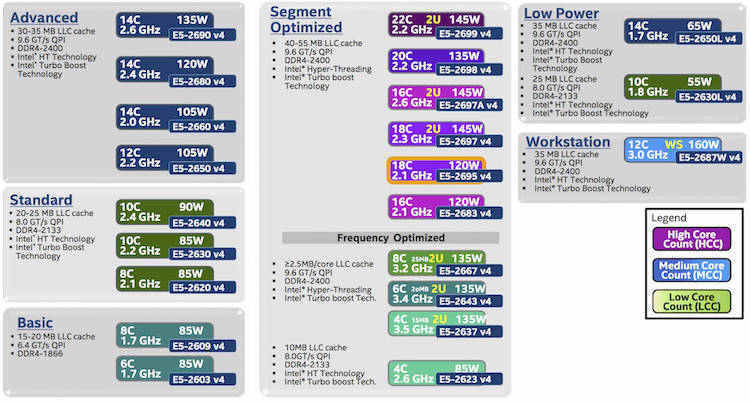
The Segment Optimized features a sub segment of Frequency Optimized, these CPU’s push the gigabit boundaries. And then off course there is the custom-build segment, which is off the list, but if you have enough money, Intel can look into your problems. The most popular CPUs used in the virtual datacenter come from the advanced and segment optimized segments. These CPUs provide enough cores and cache to drive a healthy consolidation ratio. Primarily the high core count CPUs from the Segment Optimized category are used. All CPU’s from these segments are equipped with a QPI link speed of 9.6 GT/s.
| Segment | Model Number | Core count | Clock cycle | TDP | QPI speed |
|---|---|---|---|---|---|
| Advanced | E5-2650 v4 | 12 | 2.2 GHz | 105W | 9.6 GT/s |
| Advanced | E5-2660 v4 | 14 | 2.0 GHz | 105W | 9.6 GT/s |
| Advanced | E5-2680 v4 | 14 | 2.4 GHz | 120W | 9.6 GT/s |
| Advanced | E5-2690 v4 | 14 | 2.6 GHz | 135W | 9.6 GT/s |
| Optimized | E5-2683 v4 | 16 | 2.1 GHz | 120W | 9.6 GT/s |
| Optimized | E5-2695 v4 | 18 | 2.1 GHz | 120W | 9.6 GT/s |
| Optimized | E5-2697 v4 | 18 | 2.3 GHz | 145W | 9.6 GT/s |
| Optimized | E5-2697A v4 | 16 | 2.6 GHz | 145W | 9.6 GT/s |
| Optimized | E5-2698 v4 | 20 | 2.2 GHz | 135W | 9.6 GT/s |
| Optimized | E5-2699 v4 | 22 | 2.2 GHz | 145W | 9.6 GT/s |
QPI Link Speed Impact on Performance
When opting for a CPU with a lower QPI link speeds, remote memory access will be impacted. During the tests of QPI bandwidth using the Intel Memory Latency Checker v3.1. it reported an average of ˜75% of the theoretical bandwidth when fetching memory from the remote NUMA node.
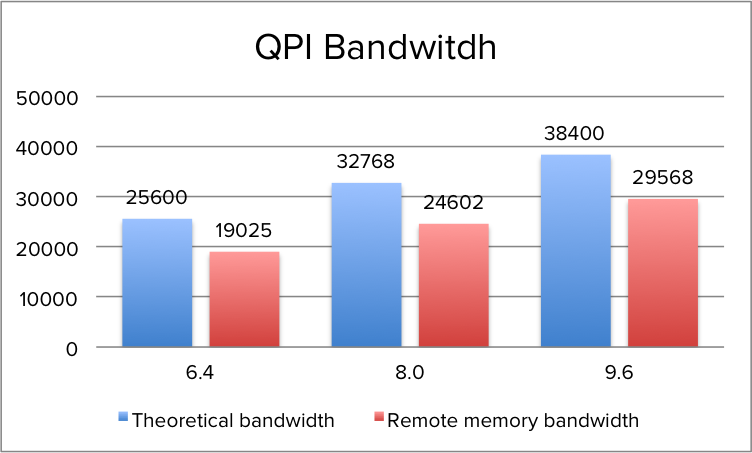
The peak bandwidth is more a theoretical maximum number as transfer data comes with protocol overhead. Additionally tracking resources are needed when using multiple links to track each data request and maintain coherency. The maximum QPI bandwidth that is available at the time of writing is lower than the minimum supported memory frequency of 1600 MHz (Intel Xeon v3 & v4). The peak bandwidth of DDR4 1600 MHz is 51 GB/s, which exceeds the theoretical bandwidth of the QPI by 32%. As such, QPI bandwidth can impact remote memory access performance. In order to obtain the most performance, it’s recommended to select a CPU with a QPI configuration of 9.6 GT/s to reduce the bandwidth loss to a minimum, the difference between 9.6 GT/s and 8.0 GT/s configuration is a 29% performance drop. AS QPI bandwidth impacts remote memory access, it’s the DIMM configuration and memory frequency that impacts local memory access. Local memory optimization is covered in Part 4.
Note!
The reason why I’m exploring nuances of power settings is that high-performance power consumption settings are not always the most optimal setting for today’s CPU microarchitecture. Turbo mode allows cores to burst to a higher clock rate if the power budget allows it. The finer details of Power management and Turbo mode are beyond the scope of this NUMA deep dive, but will be covered in the upcoming CPU Power Management Deep Dive.
Intel QPI Link Power Management
Some servers allow you to configure the QPI Link Power Management in the BIOS. When enabled, the buffers in the QPI links are allowed to enter a sleep state when the links are not being used. When there is relatively little traffic, the QPI link shuts down some of its data transmissions lanes, this to achieve power consumption reduction. Within a higher state, it only reduces bandwidth, when entering a deeper state memory access will occur latency impact.
A QPI link consists of a transmit circuit (TX), 20 data lanes, 1 clock lane and a receive circuit (RX). Every element can be progressively switched off. When the QPI is under heavy load it will use all 20 lanes, however when experiencing a workload of 40% or less it can decide to modulate to half width. Half width mode, called L0p state saves power by shutting down at least 10 lanes. The QPI power management spec allows to reduce the lanes to a quarter width, but research has shown that power savings are too small compared to modulating to 10 links. Typically when the 10 links are utilized for 80% to 90% the state shifts from L0p back to the full-width L0 state. L0p allows the system to continue to transmit data without any significant latency penalty. When no data transmit occurs, the system can invoke the L0s state. This state only operates the clock lane and its part of the physical TX and RX circuits, due to the sleep mode of the majority of circuits (lane drivers) within the transceivers no data can be sent. The last state, L1, allows the system to shut down the complete link, benefitting from the highest level of power consumption.
L0s and L1 states are costly from a performance perspective, Intel’s’ patent US 8935578 B2 indicates that exiting L1 state will cost multiple microseconds and L0s tens of nanoseconds. Idle remote memory access latency measured on 2133 MHz memory is on average 130 nanoseconds, adding 20 nanoseconds will add roughly 15% latency and that’s quite a latency penalty. A low power state with longer latency and lower power than L0s and is activated in conjunction with package C-states below C00
| State | Description | Properties | Lanes |
|---|---|---|---|
| L0 | Link Normal Operational State | All lanes and Forward Clock active | 20 |
| L0p | Link power saving state | A lower power state from L0 that reduces the link from full width to half width | 10 |
| L0s | Low Power Link State | Turns odd most lane drivers, rapid recovery to the L0 state | 1 |
| L0s | Deeper Low Power State | Lane drivers and Fwd clock turned off, greater power savings than L0s, Longer time to return to L0 state |
If the focus is on architecting a consistent high performing platform, I recommend to disable QPI Power Management in the BIOS. Many vendors have switched their default setting from enabled to disabled, nevertheless its wise to verify this setting.
The memory subsystem and the QPI architecture lay the foundation of the NUMA architecture. Last level cache is a large part of the memory subsystem, the QPI architecture provides the interface and bandwidth between NUMA nodes. It’s the cache coherency mechanisms that play a great part in providing the ability to span virtual machines across nodes, but in turn, will impact overall performance and bandwidth consumption.
Up next, Part 3: Cache Coherency
The 2016 NUMA Deep Dive Series:
Part 0: Introduction NUMA Deep Dive Series
Part 1: From UMA to NUMA
Part 2: System Architecture
Part 3: Cache Coherency
Part 4: Local Memory Optimization
Part 5: ESXi VMkernel NUMA Constructs
Part 6: NUMA Initial Placement and Load Balancing Operations
Part 7: From NUMA to UMA

Great article Frank! I’m writing a similar set of articles more focused around Desktop Virtualisation for both RDSH and VDI workloads.
For the Coreinfo screen shot that shows two NUMA nodes presented to the Windows VM, was that VM configured with 12 sockets x 1 core or 2 sockets x 6 cores?
Cheers,
Jeremy
Cool stuff! I can imagine you want to do it as well. Although low-level functionality is the same for VDI as well as for Server virtualization or bare metal workload it’s fun researching all this stuff thoroughly instead of creating another copy or just blatantly rip off someone else their work.
Well…the different hypervisors seem to behave differently when it comes to NUMA. I’m only interested in ESX, Hyper-V and XenServer. And then you’ve got Cluster-On-Die (COD) to consider, and then understanding the QPI snoop modes and how they differ between Haswell and Broadwell. Also how hyper-threading and over-committing pCPU ties into it all. I agree, the research is fun. Trying to get information from Intel is like pulling hens teeth…but still fun 🙂
Yeah true about the hypervisor operations, but the first four parts concentrate mostly on hardware level operations. Snoop modes and Cluster on Die are covered in part 3, which is scheduled to appear today or tomorrow. Intel has got these amazing reference architecture documents, which is loaded with top-notch information. The developer forums are also an amazing resource with people such as Dr. Calpin as regular contributors. And It does help though when you are in the position to talk to the lead engineers of the Xeon line :).
🙂 I kept coming up against road blocks. Intel staff in APAC are unresponsive and unhelpful. Are those reference architecture documents public?
Try this one: http://www.intel.nl/content/dam/www/public/us/en/documents/manuals/64-ia-32-architectures-optimization-manual.pdf
Awesome…thanks Frank. There is some sensational information in there. This is a new reference architecture only released in June. My research was in Q1 this year. Damn…I was too early and Intel were so unhelpful at the time.
Listed as 9.6 GT/s a QPI link can transmit up to 19.2 MB/s from one CPU to another CPU. (I think you mean 19.2 GB/s)
Thanks Philippe for spotting the typo. You are right, I meant GB/s instead of MB/s.I fixed it.
Thanks frank for all this stuff, I have a few questions about the Broadwell HCC Architecture diagram.
1. Why is there 2 ring ?
2. As the Intel Broadwell contains 4 memory channels, is the SMI components handle one memory channels each ?
3. When I look at the purple path on the diagram, I think that based on the flows the core 00 has to “give” data to the core 02, the core 02 to the core 04, and so on, to access the QPI agent ?
4. In the last table, the QPI power states, I think that the last one is not L0s but L1 🙂